
This page might be of some use to owners of the Aztech DSL600E, or the Solwise SAR-600E, which is the same thing, who are trying to figure out what is connected to what in order to modify the hardware or whatever. It includes images of the PCB and pin assignments for the serial and JTAG headers. Also see this page for an annotated 4800dpi scan of the underside of the CPU area.
Here is a 1200dpi scan of the PCB out of my SAR-600E (note that it says DSL600E on it, because they are the same thing). Click the image for the full-size version, which is fucking huge. I reckon it's a lot easier to see stuff on that than it is looking at the real thing. A scanner is a fucking excellent microscope sometimes.
I haven't done a scan of the upper side, partly because it has tall components on it so it'd probably be out of focus, and partly because there are so many components on it that you can't see fuck all anyway. I have taken a photo though, which has come out as crappily as I have come to expect from my crappy digital camera. Click on it for the full size version.

There follow some pictures of the various headers for which space is available on the board, with their pin assignations. Note that these are all from the UNDERSIDE of the board, and so are reversed left-to-right compared to looking at the side you'd actually solder the headers to if you were to install them.
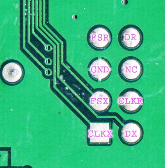
This picture shows the pin assignations for the 8-pin header J7. This is a serial interface of some unusual nature used by various TI chips. This PDF describes its operation in the TMS320C31.
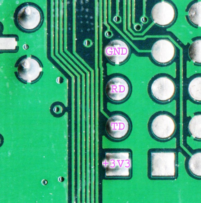
This picture shows the pin assignments for the 4-pin header J4. This is the RS232 serial port. This is the only header that is actually installed as standard.
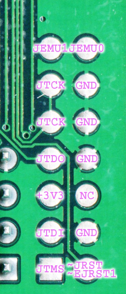
This picture shows the pin assignments for the 14-pin header J6. This is one of the two JTAG ports. I think this port is for the DSP core alone; for some reason there are separate ports for the DSP and MIPS cores. It appears to be a standard pinout except that JEMU0 and JEMU1 are the wrong way round, but that might not even be right anyway.
I believe the following is a valid mapping to create a Xilinx DLC5 type unbuffered JTAG cable, though I have not tested it as yet because I am still waiting for the connectors to arrive.
| JTAG signal | LPT signal | LPT pin |
|---|---|---|
| TDI | D0 | 2 |
| TDO | SEL | 13 |
| TMS | D2 | 4 |
| TCLK | D1 | 3 |
| GND | GND | 18-25 |
It may also be necessary to pull ~TRST high. It has a 4k7 pulldown on the PCB so anything between 100 ohms and 1k ought to do for a pullup. TI actually say not to do this, but numerous reports on the web say it doesn't work if you don't. We shall see. ~SRST has a 4k7 pullup on the PCB and can apparently be ignored.
This PDF by TI about JTAG may also be of interest.
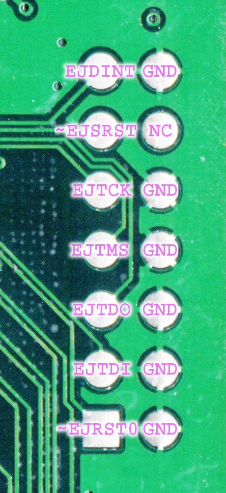
This picture shows the pin assignments for the 14-pin header J3. This is the JTAG port for the MIPS core. It is an EJTAG port, but it is not standard - the pin which is supposed to be +ve is actually ground. The rest of it appears to be standard, although I am not sure about the positions of the top two pins - they might be the wrong way round. This is because they have not been experimentally verified. Trying to trace the PCB tracks it looks like the pins are in a totally scrambled order, but connecting a JTAG cable accordingly does not work at all, whereas connecting it according to the standard order does work; but my cable, like most, does not make use of those pins, so they remain untested.
Back to AR7 Index
Back to Pigeon's Nest
Be kind to pigeons
![]()